Topological Insulators
Bismuth selenide insulates inside and conducts on every surface. Its surface electrons form a cone, their spin locked to their motion.
Chapters · 17
- 01One cone
- 02A third kind of solid
- 03Layers of five
- 04Cut open: insulating inside, a conducting skin
- 05The Dirac cone
- 06Spin locked to momentum
- 07No turning back
- 08Bands turned over
- 09Light in, electrons out
- 10Cut open: the analyser
- 11A clean, cold surface
- 12A slice of the cone
- 13The first experiments
- 14The inside still conducts
- 15Quantum Hall, no magnet
- 16Taken apart
- 17Trace a cone
Scroll
One cone
In a measurement published in 2009, researchers put a crystal of bismuth selenide (Bi₂Se₃) in ultra-high vacuum, split it open at 10 to 55 K, shone ultraviolet light from a synchrotron on the fresh surface and measured the electrons it knocked out. The surface electrons’ energy rose in a straight line with their momentum: drawn out, a cone, with an upside-down cone below it, tip to tip. The whole surface had just this one cone.
The measurement resolved energies to 15 meV and momenta to 1.5 % of the surface Brillouin zone. The cone’s slope is the surface electrons’ speed, about 500,000 m/s, about a six-hundredth of the speed of light. Inside the crystal there is a gap of about 0.3 eV between the bands, and the surface cone runs straight across it.
One Dirac cone · 15 meV · surface electrons about 5 × 10⁵ m/s (2009)
A third kind of solid
Electrons in a solid can only have energies within certain ranges, called bands. In an insulator the electrons exactly fill some bands, and the next empty band lies above a gap, so it takes a lot of energy to set them moving: no current. In a metal the highest band is only partly filled, and the smallest push sets electrons moving.
Inside, a topological insulator is like an insulator: there are no states for electrons in the gap. But on every surface some states run right across the gap, joining the band below to the band above, so the surface conducts. These surface states are not like an ordinary metal either: in a metal each momentum has two states, spin up and spin down; here there is one, like half a metal.
Insulator: a gap · metal: a half-filled band · topological insulator: surface states cross the gap
Layers of five
Bismuth selenide is built of layers of atoms. Each layer is a triangular net with neighbours 4.143 Å apart (an ångström is a ten-billionth of a metre). The layers come in fives: selenium, bismuth, selenium, bismuth, selenium, held firmly together by chemical bonds. Between one group and the next there are only much weaker van der Waals forces, and a gap: the selenium layers on either side are 2.58 Å apart.
A group of five is 6.97 Å thick from the selenium on one side to the selenium on the other, and with one gap it repeats every 9.545 Å; three groups make one unit cell 28.636 Å tall. These numbers come from X-ray diffraction in 1963. The crystal splits easily along the gaps between the groups, leaving a flat surface paved with selenium atoms.
Se–Bi–Se–Bi–Se · 6.97 Å a group · 2.58 Å between groups · repeats every 9.545 Å
Cut open: insulating inside, a conducting skin
The copper layer of the model marks how deep the surface states reach. By first-principles calculations, near the tip of the cone they lie within about the outer two groups, about 2 nm; further from the tip they reach deeper. They are on every face: the top, the bottom and the sides. The dark part deep inside has no such states.
Why must the surface conduct? Ordinary insulators, vacuum included, have their bands in the “normal” order; inside a topological insulator the order is “turned over” (see “Bands turned over” below). Going from inside to outside the order has to change back, so the gap has to close at the boundary, and the surface must carry states that cross the gap; as long as nothing magnetic is there, no change to the surface can remove them. Split the crystal along a gap and the new face has them at once.
Surface states: about 2 nm (calculated) · on every face · the colour marks depth only; the atoms are the same as inside
The Dirac cone
Plot the surface electrons’ energy above their momentum and you get the cone: energy changes in a straight line with the size of the momentum, E = ħvk. The tip is called the Dirac point. “Dirac” refers to the equation behind this shape, which has the same form as Dirac’s equation for massless relativistic particles; the electrons are ordinary electrons, moving at about 500,000 m/s, less than two thousandths of the speed of light.
Graphene has cones like this too, four of them (two places, each with two spins). One surface of bismuth selenide has a single one, a quarter of graphene. By theory a lone cone like this cannot appear in a two-dimensional material on its own; its partner is on the crystal’s opposite surface.
E = ħvk · ħv ≈ 3.3 eV·Å · about a quarter of graphene
Spin locked to momentum
On the surface each momentum comes with one spin direction only: the spin lies in the surface, at right angles to the motion. An electron moving the opposite way has the opposite spin. Going once round a ring of the cone, the spin turns round once too.
In bismuth selenide and its relatives, seen from above the surface, the spins above the tip of the cone run round clockwise, and below it anticlockwise. In 2009 researchers fitted Mott detectors behind the analyser, counted the electrons by spin, and saw the locking directly. How strongly the spins are polarised differs between measurements and calculations: about 50 % by calculation, about 75 % measured on bismuth selenide in 2011.
Spin ⟂ momentum · clockwise above the tip, anticlockwise below (seen from above)
No turning back
An electron that meets an impurity can be thrown in many directions, one of them straight back. On this surface the state going straight back has exactly the opposite spin, and an impurity that is not magnetic cannot flip a spin, so that one path is closed. The more two states’ spins differ, the harder the scattering: for an ideal cone the chance of turning through an angle θ goes as cos²(θ/2), half at 90°, zero at 180°.
In 2009 two groups used scanning tunnelling microscopes to look at the electron waves round impurities on bismuth–antimony and bismuth telluride, and found no sign of scattering straight back. The surface is not free of resistance for that: scattering through other angles still happens, and the electrons wander. In the quantum Hall effect the electrons on an edge can only go one way (see the “Quantum Hall Effect” plate); here they can go both ways, they just cannot retrace their path.
Chance of turning through θ ∝ cos²(θ/2) · zero at θ = 180° · except for magnetic impurities
Bands turned over
Bismuth has atomic number 83: it is heavy. In heavy atoms an electron’s spin is strongly coupled to its motion round the nucleus, called spin–orbit coupling. By a 2009 calculation, where the momentum in bismuth selenide is zero the two levels nearest the Fermi energy have opposite parity; spin–orbit coupling pushes one down and the other up, and at about 60 % of its real strength the two swap places: the bands are turned over.
Bands turned over cannot be changed back by small steps without the gap closing on the way. Theory tells the two kinds of insulator apart with a number that is 0 or 1 (the Z₂ invariant): proposed for two dimensions in 2005, extended to three in the summer of 2006 by three groups on their own, when the name “topological insulator” was coined. “Topological” is about this property of the bands, not about the crystal’s shape: a cube or a flake of bismuth selenide is the same.
Bismuth: Z = 83 · bands swap at about 60 % of the real spin–orbit coupling (calculated) · Z₂ = 0 or 1
Light in, electrons out
The cone is seen with angle-resolved photoemission spectroscopy, ARPES. Ultraviolet light falls on the sample and an electron takes up one photon’s energy and flies out: the photoelectric effect, found by Hertz in 1887 and explained by Einstein in 1905. The electron leaves with kinetic energy E_kin = hν − φ − |E_B|: the photon’s energy, less the work function it pays to leave the surface, less the binding energy it had in the crystal.
The direction it flies off in gives its momentum along the surface: k∥ = 0.512 √E_kin · sin θ (momentum in Å⁻¹, energy in eV). Crossing the surface, the momentum along it is kept while the part across it changes, so states that move only in the plane, like surface states, are the best to measure this way. Laboratories often use a helium lamp, whose brightest line gives photons of 21.218 eV; a synchrotron’s photon energy can be tuned.
E_kin = hν − φ − |E_B| · k∥ = 0.512 √E_kin sin θ · helium lamp 21.218 eV
Cut open: the analyser
The electrons first pass a set of electrostatic lenses. The lens images electrons leaving at different angles onto different points along the entrance slit, and slows them to a fixed “pass energy”. A typical lens takes in electrons within ±15° at once, resolving angles down to about 0.1°.
Then the electrons enter the space between two concentric hemispheres. A voltage between them sends electrons with exactly the pass energy half way round on the mean radius, often 200 mm; slightly faster ones swing wider and slower ones tighter, so at the exit they are spread out by energy. The energy resolution is about pass energy × slit width ÷ (2 × mean radius): with 20 eV and a 0.2 mm slit, about 10 meV.
Mean radius 200 mm · ΔE ≈ E_p · w / 2R₀ · 20 eV, 0.2 mm → about 10 meV
A clean, cold surface
Photoelectrons escape only from the top few layers: at the usual energies an electron goes about 5 Å in a solid before it is scattered, so ARPES sees almost nothing below the top group of five. The surface must be very clean: as a rule of thumb, at a millionth of a torr a layer of gas molecules settles on a surface in about a second. During measurements the chamber is held below 5 × 10⁻¹¹ torr, and the sample is split only once it is inside; in 2009 the crystals were split in place at 10 to 55 K.
The sample sits at the end of a manipulator that comes down from the top, moves along three directions and turns about three axes, with liquid helium flowing through it; it routinely reaches about 10 K, so that heat does not blur the states near the Fermi energy. The direction an electron flies to the analyser is the data, so no magnetic field may bend it: the chamber is lined with mu-metal to bring the field at the sample below 100 nT, against the Earth’s 30 to 60 µT.
Below 5 × 10⁻¹¹ torr · about 10 K · field at the sample ≤ 100 nT
A slice of the cone
At the hemispheres’ exit is the detector: two microchannel plates turn each electron into about a million, which strike a phosphor screen and make it glow, and a camera records the screen. One commercial analyser’s plates are 40 mm across. One direction on the screen is energy, the other the angle along the slit, so each frame is a picture of energy against momentum.
If the slit passes through the tip of the cone, the image is an X, its upper half cut off at the Fermi energy; a little to one side, it becomes a hyperbola. Turn the sample and record slice after slice, and the whole cone is built up; laid side by side at one energy, they give a ring, the “Fermi surface”. The laboratory below does just this.
Two microchannel plates + phosphor screen + camera · energy one way, angle the other
The first experiments
In 2006 theory predicted that mercury telluride quantum wells thick enough would become two-dimensional topological insulators. In 2007 an experiment found conduction along the edges of wells thicker than 6.3 nm: at 30 mK, devices 1 µm long had a conductance close to 2e²/h, whatever their width.
The first three-dimensional one was bismuth–antimony: in 2008 ARPES counted 5 surface states crossing the Fermi energy on Bi₀.₉Sb₀.₁, an odd number, which marks it as topological; but its surface states were complicated and its gap small. In 2009 calculations predicted that bismuth selenide, bismuth telluride and antimony telluride are topological insulators with a single cone on the surface, and in the same year ARPES saw that cone on bismuth selenide and on bismuth telluride.
2007: mercury telluride quantum wells · 2008: bismuth–antimony · 2009: bismuth selenide, bismuth telluride
The inside still conducts
In real bismuth selenide some places where selenium atoms belong are always empty. These defects give up electrons: crystals as grown typically have about 10¹⁹ extra electrons per cm³, the Fermi energy lies in the conduction band, and the inside is in fact a metal. In 2010 such a crystal’s Fermi energy was measured 150 meV above the bottom of the conduction band, about 340 meV above the Dirac point. In a resistance measurement most of the current then goes through the inside, and the surface’s share is swamped.
The answers are new recipes and thin films. A little calcium in bismuth selenide cancels the extra electrons. In bismuth telluride selenide (Bi₂Te₂Se) the selenium sits in the middle of each group of five, where it is hard to lose, and the resistivity exceeds 1 Ω·cm: at 1.6 K about 6 % of a 260 µm crystal’s conductance comes from the surface, against about 0.3 % for bismuth telluride. Films can be grown too, but in bismuth selenide thinner than 6 groups the top and bottom surfaces couple and a gap opens at the tip of the cone, about 0.25 eV at 2 groups.
About 10¹⁹ electrons per cm³ · Fermi energy 150 meV into the conduction band · a gap below 6 groups
Quantum Hall, no magnet
Magnetism breaks time-reversal symmetry: the path straight back is no longer closed, and a gap can open at the tip of the cone. In 2010 a gap of about 50 meV was measured on iron-doped bismuth selenide; where such gaps come from, though, later experiments dispute.
In 2013 researchers grew chromium-doped (Bi,Sb)₂Te₃ as a film 5 groups thick, cooled it to 30 mK and, with no magnetic field, found the Hall resistance settled on h/e² (about 25,813 Ω): the quantum anomalous Hall effect. Current flows one way along the film’s edges, as in the quantum Hall effect, only without an outside magnetic field (see the “Quantum Hall Effect” plate). The resistance along the film was still 0.098 h/e² then. In 2020 the effect appeared at 1.4 K in MnBi₂Te₄, a material that is magnetic itself.
30 mK · zero field · Hall resistance h/e² · chromium-doped (Bi,Sb)₂Te₃, 5 groups thick (2013)
Taken apart
The helium lamp, the manipulator with its cold head, the electrostatic lens, the analyser’s housing and the two hemispheres inside it, the detector with its camera, the turbo pump and the ion pump come apart one by one.
Rest the pointer on a part (tap it on a phone) and that part lifts on its own and is named; the rest fade.
Trace a cone
The lever turns the sample’s tilt, so the slit sweeps across the other direction of momentum: for electrons at the Fermi energy k_y = 0.512 √E_kin · sin(tilt), worked out here with the helium lamp’s 21.218 eV and a work function of 4.5 eV that this page assumes. At the Fermi energy the cone is about 0.1 Å⁻¹ across in radius, only about 3° of emission angle.
The picture is the slice the detector records at this tilt. At zero tilt the slit passes through the tip and the slice is an X; tilt further and the two branches part into a hyperbola; beyond about 3° the upper branch lies wholly above the Fermi energy and is gone. The picture is this page’s sketch from the cone’s speed and the energies measured in 2010, not measured data.
Try thisTurn the sample’s tilt slowly from 0° to 4°: how do the two crossings at E_F move? At what tilt do they meet, and then vanish?
What the model leaves out
The crystal’s atoms are placed from 1963 X-ray diffraction, and the groups of five and the gaps between them are to scale; the atoms’ size is the model’s, and they are shown only on exposed faces, the slabs being solid inside. The model has 8 groups and is about 9 nm across; a real crystal is millimetres thick. The copper marks only the depth of the surface states (drawn as about 2 nm); the atoms there are bismuth and selenium like those inside. The model is cut open only to show the inside; if a real crystal were cut, the new face would carry surface states too. The blue beads are sketched surface electrons, much slowed, the red arrows their spins, and their scattering angles are drawn from cos²(θ/2). The band model’s cone is drawn at 5 × 10⁵ m/s; the Dirac point 340 meV below the Fermi energy and the bottom of the conduction band 190 meV above it are the 2010 measurement’s; the top of the valence band is this page’s estimate from a gap of about 0.3 eV; the bulk bands are drawn as bowls, only a sketch. The magnetic gap is drawn as 50 meV. The ARPES bench is drawn at 1:4 in a common layout, not from any laboratory’s or maker’s plans: the chamber 306 mm across, the hemispheres’ mean radius 200 mm, the lens tip 34 mm from the sample and the capillary about 5 mm from it are published figures; other sizes are estimates, and the hemispheres’ radii are a sketch. Light and electrons are much slowed, and the electrons’ paths in the analyser exaggerate their energy differences. The band maps, the screen’s image and the laboratory’s readouts are computed by this page from the model, with a work function of 4.5 eV; they are not measured data. The small figure of band inversion is a two-band toy model.
Common misconceptions
“The inside of a topological insulator is a perfect insulator” is not right: in theory it is, but real bismuth selenide often conducts inside because of defects. “Surface electrons never scatter and have no resistance” is not right: they cannot retrace their path, but they scatter in other directions; one-way edge currents without losses belong to the quantum Hall and quantum anomalous Hall effects. “Topological is about the crystal’s shape, like a doughnut” is not right: it is about the bands in momentum space. Nor does the spin point along the motion: it is at right angles to it. “Electrons in a Dirac cone are massless and move like light” is not right: the cone only relates energy and momentum, and the electrons move at about a six-hundredth of the speed of light. Nor is the cone a shape in space: across is momentum, up is energy. ARPES does not photograph electrons: it measures the energy and direction of the electrons that escape; the hemispherical analyser sorts them by energy, while the lens images their direction. The surface spin polarisation is not “100 %”: measurements and calculations give different values. The 2016 Nobel Prize in Physics was for the theory of topological phase transitions and topological phases of matter, not for topological insulators themselves. Majorana particles on topological-insulator surfaces are a 2008 proposal; a 2017 paper claiming “chiral Majorana” modes was retracted in 2022. A very thin film is no longer a three-dimensional topological insulator: bismuth selenide thinner than 6 groups has a gap at the tip of the cone.
Common questions · 4
- What is a topological insulator?
Inside, a topological insulator is like an insulator: there are no states for electrons in the gap. But on every surface some states run right across the gap, joining the band below to the band above, so the surface conducts.
02A third kind of solid ↑- What is spin–momentum locking?
On the surface each momentum comes with one spin direction only: the spin lies in the surface, at right angles to the motion.
06Spin locked to momentum ↑- Why can’t surface electrons turn straight back?
On this surface the state going straight back has exactly the opposite spin, and an impurity that is not magnetic cannot flip a spin, so that one path is closed.
07No turning back ↑- What does one ARPES image show?
One direction on the screen is energy, the other the angle along the slit, so each frame is a picture of energy against momentum.
12A slice of the cone ↑
Sources
- M. Z. Hasan, C. L. Kane (2010): Colloquium: Topological insulators, Rev. Mod. Phys. 82, 3045 (the band picture; why the surface must conduct; half a metal; diffusive, not ballistic)
- X.-L. Qi, S.-C. Zhang (2011): Topological insulators and superconductors, Rev. Mod. Phys. 83, 1057 (the spins’ handedness; topological equivalence)
- Y. Ando (2013): Topological Insulator Materials, J. Phys. Soc. Jpn. 82, 102001 (10¹⁹ electrons per cm³; Bi₂Te₂Se; cleaving between groups of five)
- C. L. Kane, E. J. Mele (2005): Z₂ Topological Order and the Quantum Spin Hall Effect, PRL 95, 146802
- L. Fu, C. L. Kane, E. J. Mele (2007): Topological Insulators in Three Dimensions, PRL 98, 106803
- J. E. Moore, L. Balents (2007): Topological invariants of time-reversal-invariant band structures, PRB 75, 121306
- R. Roy (2009): Topological phases and the quantum spin Hall effect in three dimensions, PRB 79, 195322
- B. A. Bernevig, T. L. Hughes, S.-C. Zhang (2006): Quantum Spin Hall Effect and Topological Phase Transition in HgTe Quantum Wells, Science 314, 1757
- M. König et al. (2007): Quantum Spin Hall Insulator State in HgTe Quantum Wells, Science 318, 766 (6.3 nm; 2e²/h; 30 mK)
- D. Hsieh et al. (2008): A topological Dirac insulator in a quantum spin Hall phase, Nature 452, 970 (Bi₀.₉Sb₀.₁; five surface states)
- H. Zhang et al. (2009): Topological insulators in Bi₂Se₃, Bi₂Te₃ and Sb₂Te₃ with a single Dirac cone on the surface, Nature Physics 5, 438 (band inversion; about 60 %; 0.3 eV)
- Y. Xia et al. (2009): Observation of a large-gap topological-insulator class with a single Dirac cone on the surface, Nature Physics 5, 398 (bismuth selenide; 15 meV; 1.5 %; about 5 × 10⁵ m/s; split at 10–55 K)
- Y. L. Chen et al. (2009): Experimental Realization of a Three-Dimensional Topological Insulator, Bi₂Te₃, Science 325, 178 (a quarter of graphene)
- D. Hsieh et al. (2009): A tunable topological insulator in the spin helical Dirac transport regime, Nature 460, 1101 (spins measured with Mott detectors)
- W. Zhang et al. (2010): First-principles studies of the three-dimensional strong topological insulators Bi₂Te₃, Bi₂Se₃ and Sb₂Te₃, New J. Phys. 12, 065013 (about 2 nm)
- Y. Zhang et al. (2010): Crossover of the three-dimensional topological insulator Bi₂Se₃ to the two-dimensional limit, Nature Physics 6, 584 (a gap below 6 groups)
- P. Roushan et al. (2009): Topological surface states protected from backscattering by chiral spin texture, Nature 460, 1106
- T. Zhang et al. (2009): Experimental Demonstration of Topological Surface States Protected by Time-Reversal Symmetry, PRL 103, 266803
- Y. L. Chen et al. (2010): Massive Dirac Fermion on the Surface of a Magnetically Doped Topological Insulator, Science 329, 659 (conduction band 150 meV below E_F; a gap of about 50 meV)
- J. Sánchez-Barriga et al. (2016): Nonmagnetic band gap at the Dirac point of the magnetic topological insulator (Bi₁₋ₓMnₓ)₂Se₃, Nature Communications 7, 10559
- Z.-H. Pan et al. (2011): Electronic Structure of the Topological Insulator Bi₂Se₃ Using ARPES: Evidence for a Nearly Full Surface Spin Polarization, PRL 106, 257004 (about 0.75)
- O. V. Yazyev, J. E. Moore, S. G. Louie (2010): Spin Polarization and Transport of Surface States in the Topological Insulators Bi₂Se₃ and Bi₂Te₃ from First Principles, PRL 105, 266806 (about 50 %)
- Y. S. Hor et al. (2009): p-type Bi₂Se₃ for topological insulator and low-temperature thermoelectric applications, PRB 79, 195208 (calcium doping)
- Z. Ren et al. (2010): Large bulk resistivity and surface quantum oscillations in the topological insulator Bi₂Te₂Se, PRB 82, 241306 (about 6 %)
- C.-Z. Chang et al. (2013): Experimental Observation of the Quantum Anomalous Hall Effect in a Magnetic Topological Insulator, Science 340, 167 (30 mK; h/e²; 0.098 h/e²)
- Y. Deng et al. (2020): Quantum anomalous Hall effect in intrinsic magnetic topological insulator MnBi₂Te₄, Science 367, 895 (1.4 K)
- L. Fu, C. L. Kane (2008): Superconducting Proximity Effect and Majorana Fermions at the Surface of a Topological Insulator, PRL 100, 096407 (a proposal)
- Q. L. He et al. (2017): Chiral Majorana fermion modes in a quantum anomalous Hall insulator–superconductor structure, Science 357, 294 (retracted in 2022)
- S. Nakajima (1963): The crystal structure of Bi₂Te₃₋ₓSeₓ, J. Phys. Chem. Solids 24, 479 (via the Crystallography Open Database, 9011965: a = 4.143 Å, c = 28.636 Å)
- The Nobel Prize: press release, Physics 2016 (topological phase transitions and topological phases of matter)
- A. Damascelli, Z. Hussain, Z.-X. Shen (2003): Angle-resolved photoemission studies of the cuprate superconductors, Rev. Mod. Phys. 75, 473 (E_kin = hν − φ − |E_B|; about 5 Å; 5 × 10⁻¹¹ torr)
- J. A. Sobota, Y. He, Z.-X. Shen (2021): Electronic structure of quantum materials studied by angle-resolved photoemission spectroscopy, Rev. Mod. Phys. 93, 025006 (±15°; about 0.1°; 100 nT; about 10 K; plates multiply by about 10⁶)
- H. Zhang et al. (2022): Angle-resolved photoemission spectroscopy, Nature Reviews Methods Primers 2, 54 (k = 0.512 √E_k)
- T. Shimojima, K. Okazaki, S. Shin (2015): Low-temperature and high-energy-resolution laser photoemission spectroscopy, J. Phys. Soc. Jpn. 84, 072001 (ΔE ≈ E_p · w / 2r₀; 21.218 eV)
- NIST Atomic Spectra Database: the He I line at 58.4334 nm (21.218 eV)
- Scienta Omicron: VUV5k helium lamp, brochure (capillary 5 mm from the sample)
- Scienta Omicron: DA30-L analyser, brochure (working distance 34 mm; 40 mm microchannel plates)
- Scienta Omicron: magnetically shielded UHV chambers, brochure (306 mm across)
Data
The crystal’s atoms are placed from the Bi₂Se₃ structure of S. Nakajima (J. Phys. Chem. Solids 24, 479, 1963), read from the Crystallography Open Database (entry 9011965). The band map, the phosphor screen’s image, the cone, the spins, the electrons’ scattering and the analyser’s orbits are computed or drawn by this page from published numbers; they are not measured data. The ARPES bench follows the layout that laboratories and makers describe (a chamber with a cold manipulator from the top, a helium lamp, an electrostatic lens and a hemispherical analyser with a microchannel-plate detector); it is not drawn from any one laboratory’s or maker’s plans. Material presets, parts and the softbox studio of the site’s model kit are ported from AirsupHQ/machine-skill (MIT, © 2026 Air Supply Technologies Inc.).
The text, pictures and models on this page are licensed CC BY-NC 4.0: free to use and adapt for teaching and other non-commercial purposes, with credit to world.lapla.si. Third-party material listed above keeps its own licence.
Cite this plate
Laplace’s Mini World, Plate F50, “Topological Insulators”, https://world.lapla.si/en/topological/, CC BY-NC 4.0, updated 2026-10-26.
Follow the question
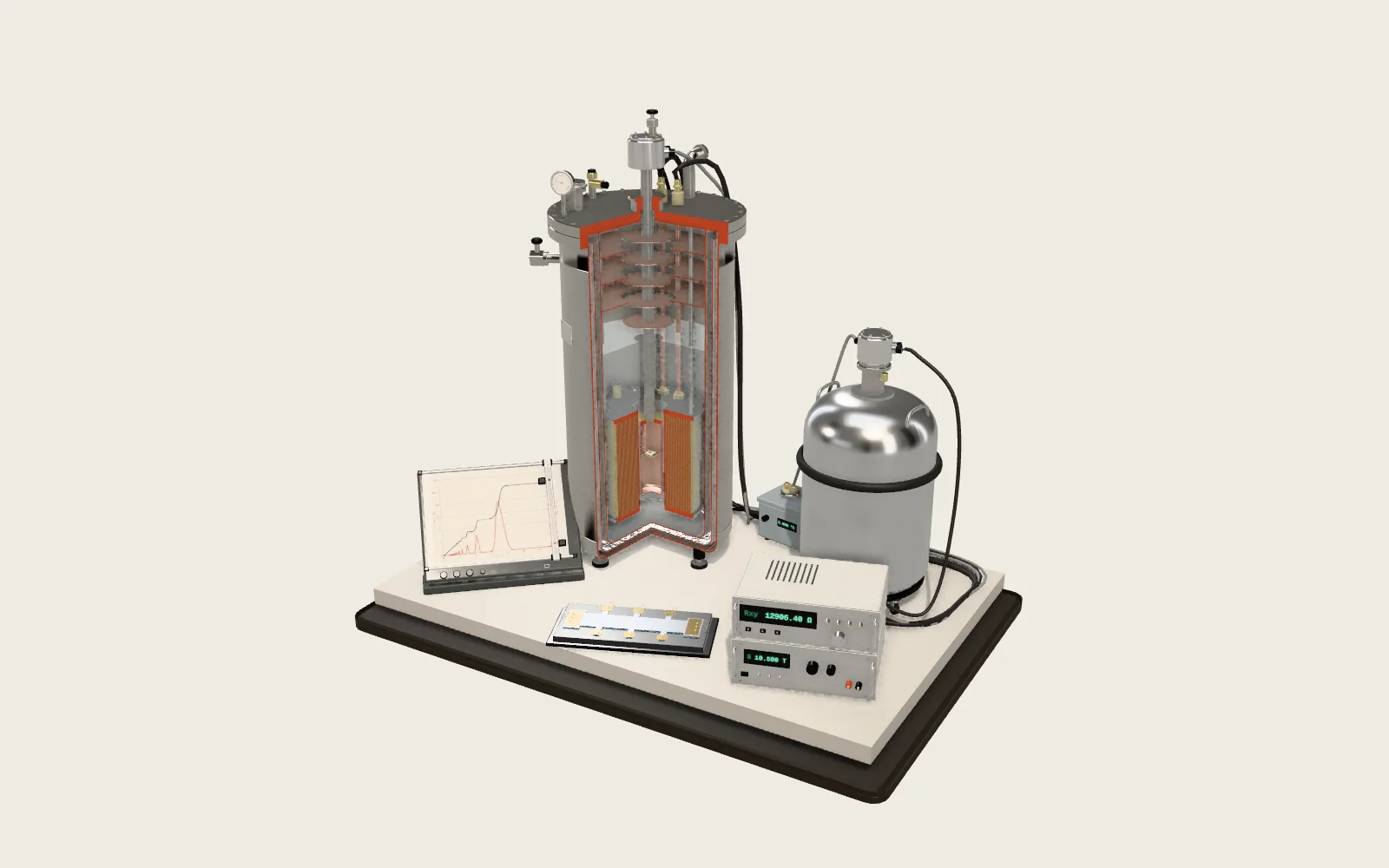 Plate F36The Quantum Hall EffectCool a sheet of electrons close to absolute zero in a strong magnetic field and its Hall resistance settles on steps set by Planck’s constant and the electron’s charge, whatever the material or shape. Metrology institutes use it to realise the ohm.
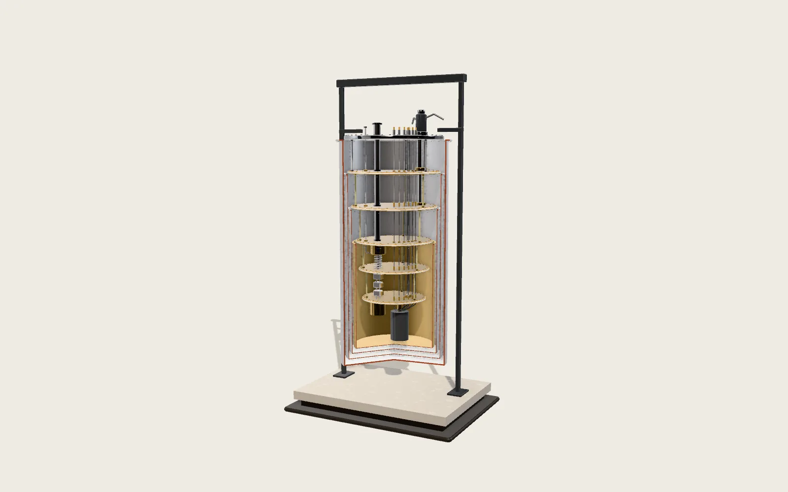 Plate F05The Dilution RefrigeratorA superconducting quantum computer hangs from a gold-plated “chandelier”. Each stage is colder than the one above; the last is about 10 mK, hundreds of times colder than space.