Gate-All-Around Transistor
As the switches in chips get shorter, their gates find it harder to hold them. The answer was to wrap the silicon: from one side, to three, to all four. A few thin sheets are stacked and the metal gate closes round each one. This is a piece of a logic cell cut open: five gates, two stacks of sheets, the source and drain crystals, contacts and the first two layers of copper.
Scroll
A Switch You Can Count in Atoms
The camera rests on the cut face of one silicon sheet. It is 5 nm thick; silicon’s lattice constant is 0.543 nm, so the sheet is about 9 unit cells, or about 37 layers of atoms, through.
The bright dots come in pairs: columns of silicon atoms seen along <110>, each pair about 0.14 nm apart. The thin amber film above and below is hafnium oxide; beyond it is the metal gate. Electrons flow along this sheet from one end to the other.
Sheet 5 nm ≈ 9 unit cells ≈ 37 atomic layers · a = 0.5431 nm
Tens of Billions on a Chip
Pull back. This piece of a cell is about 0.25 µm long. Around it are rows of cells like it; the rows make blocks, the blocks make a chip, and a few hundred chips are made together on a wafer 300 mm across.
IBM’s 2 nm gate-all-around chip, shown in 2021, could hold up to 50 billion transistors on a chip the size of a fingernail. Samsung was first into production with 3 nm gate-all-around chips, on 30 June 2022.
Wafer 300 mm · up to ~50 billion transistors on a fingernail-sized chip (IBM 2021)
The Gate Lowers a Barrier
The source is crowded with electrons; the drain sits at a positive voltage. Between them, in the silicon, lies a barrier of energy. While the electrons cannot climb it, the switch is off.
Raise the gate voltage and the barrier sinks; the electrons that get over it multiply. The ink line over the section is that barrier, computed live by the page’s model; the blue beads are electrons passing, drawn in proportion to the current.
Electrons’ energies follow Boltzmann’s distribution. At room temperature, each 60 mV or so off the barrier lets at most ten times as many over. That is the limit of the subthreshold swing: 59.5 mV per decade. Real devices are always a little slower.
Subthreshold swing ≥ (kT/q)·ln 10 = 59.5 mV/dec at 300 K
Why Wrap All Four Sides
Three transistors with the same 12 nm gate stand on one bench, each cut through the middle of its gate. The planar transistor’s gate lies on top of the silicon only. The FinFET stands the silicon up as a thin fin, gated on three sides. The gate-all-around transistor lays the silicon down in thin sheets and gates all four.
The drain’s voltage seeps into the channel from the side and helps electrons over the barrier, out of the gate’s hands. How far it reaches is set by a scale length: the more of the channel the gate wraps, and the thinner the silicon, the shorter it is. The gate has to be 5 to 10 times longer than it to switch off cleanly.
In the page’s model, the planar device’s scale length is about 5.6 nm, and a 12 nm gate cannot switch it off at all. The FinFET’s is about 2.8 nm, with a swing of about 77 mV per decade. The nanosheet’s is about 2.4 nm, with about 72 mV per decade, and more than ten times less leakage.
Scale length λ: planar 5.6 nm · fin 2.8 nm · nanosheet 2.4 nm (page model, 12 nm gate)
Cut Open
From the bottom: the silicon substrate and its shallow trench isolation; the channel of three stacked sheets; the high-k oxide and the metal gate around each one; silicon nitride spacers on both sides of the gate; the source and drain crystals grown at either end; the contacts landing on them; and above, the first and second layers of copper.
The stack in front is an n-type transistor, conducting with electrons; the one behind is p-type, conducting with holes. A pair of them is the basic unit of a CMOS circuit. The insulating oxide that fills the space between the wires has been taken out, so the structure can be seen.
Gate pitch 45 nm · gate 12 nm · three sheets, each 5 × 30 nm
Stacked Sheets
Cut across the middle of the gate and the three sheets lie one above another, each wrapped on top, bottom and both sides first in about 1.5 nm of hafnium oxide, then in the metal gate.
Round their edges, the three sheets have about 210 nm of width under the gate’s control, in a footprint 30 nm wide. Current grows with that width, so a stack drives a lot of current from a small area. The sheets can also be drawn wider or narrower, as the circuit needs.
The small white blocks between the sheets’ ends are the inner spacers. They keep the gate apart from the source and drain and cut the capacitance between them; the chapter on making shows how they get there.
Gated width 3 × 2 × (30 + 5) = 210 nm · footprint 30 nm
Build It, Then Hollow It
Floating sheets cannot be made directly. Instead, layers of silicon and silicon–germanium are grown in turn, like a layer cake; the stack is etched into narrow strips; a dummy polysilicon gate is laid across; the ends are cut away, the silicon–germanium is etched back a little from the sides and the gaps filled with inner spacers; then the source and drain crystals are grown.
Next the dummy gate is removed, and an etch that attacks silicon–germanium but not silicon hollows out every silicon–germanium layer, leaving the sheets hanging between source and drain. This is the channel release. Finally a film of hafnium oxide is laid along the gaps and metal fills them, and the gate closes round every sheet.
Stack → strips → dummy gate → cut → inner spacers → source/drain → open → release → high-k → metal gate
“2 nm” Is Not 2 nm
A chip’s “so many nanometres” has long been the name of a generation, not the size of anything on it. In the 2022 International Roadmap for Devices and Systems (IRDS), the generation called “2 nm” has a gate pitch of 45 nm, a tightest metal pitch of 20 nm and a gate length of 14 nm.
This model is built to those sizes: 45 nm between gate centres, a 12 nm gate, sheets 5 nm thick. Nothing on the transistor is 2 nm.
IRDS 2022: “2 nm” = G45M20 (gate pitch 45 nm, metal pitch 20 nm)
What Comes Next
The forksheet puts an insulating wall between the n-type and p-type stacks so they can sit closer. imec’s devices of 2021 had just 17 nm between the two.
The complementary FET (CFET) stacks the n-type transistor on top of the p-type, two transistors in one footprint. In 2023 Intel showed stacked devices at a 60 nm gate pitch and TSMC at 48 nm, both with n-type on top.
Backside power moves the power lines from above the transistors to the back of the substrate, feeding them from below through tiny vias, so the wiring above carries only signals. Intel’s 18A already uses it (PowerVia); TSMC planned volume production of its A16 for 2026, since reported as moving to 2027.
Forksheet · complementary stack (n over p) · backside power
Taken Apart
The layers slide apart vertically: substrate, isolation, source and drain, sheets, hafnium oxide, metal gate, spacers, contacts, two layers of copper. Rest the pointer on one and it is lifted out on its own and named.
Bench
Pick a structure, set the gate and drain voltages, change the gate length and the sheets’ number, width and thickness. The current, the leakage, the swing and the scale length are computed live by the page’s model; the curve below is the transfer characteristic on a log scale.
Try thisShrink the gate from 12 nm to 8 nm. What happens to each structure’s swing, and which one stops switching off first?
What the model leaves out
Geometry: a generic logic cell, sized to the IRDS 2022 “2 nm” rules and IBM’s published nanosheet devices, not any one maker’s design. The sheets are drawn as rounded rectangles; real ones are rounder. The insulating oxide between the wires, most vias and the higher wiring layers are left out. Electrons are drawn as blue beads; each stands for many electrons, and their size is not to scale. Physics: scale lengths from the single- and double-gate formulas of Yan et al. (1992) and Colinge (2008); a rectangular cross-section is treated as two double gates at right angles (1/λ² = 1/λ₁² + 1/λ₂²), which is an approximation; the barrier along the channel is Young’s (1989) quasi-2D solution; the current takes the form of the virtual-source model, with an injection velocity of 9 × 10⁶ cm/s (IRDS), an equivalent oxide thickness of 0.9 nm, a long-channel threshold of 0.44 V (so the default nanosheet leaks about 10 nA per µm) and a 0.7 V supply. Not included: source and drain resistance, quantum confinement, field-dependent mobility, self-heating, gate leakage, band-to-band tunnelling, device-to-device variation. The planar device is bulk silicon doped heavily (10¹⁹ per cm³). So the currents run high; the trends and orders of magnitude are right.
Common misconceptions
“2 nm” and “3 nm” are names of generations, not gate lengths, and not the size of anything on the chip. Gate-all-around does not beat 60 mV per decade: that limit comes from the thermal spread of electrons’ energies, and only devices that switch another way (tunnelling transistors, for instance) could get round it; wrapping the gate only brings real devices closer to it. The “gate-all-around” of the 1992 paper was a thin film gated above and below, not today’s nanosheet. The ink line shows how an electron’s energy changes along the channel; it is drawn to shape, without absolute values.
Sources
- N. Loubet et al. (2017): Stacked nanosheet gate-all-around transistor to enable scaling beyond FinFET, VLSI Technology (12 nm gate, 44/48 nm gate pitch)
- IBM Research: abstract of the above
- N. Loubet et al. (2018), ECS: Si/SiGe stack, sacrificial layers, selective release, inner spacers, ~5 nm sheets
- IBM newsroom (6 May 2021): 2 nm chip, up to 50 billion transistors on a fingernail-sized chip
- Samsung newsroom (30 June 2022): 3 nm gate-all-around production begins
- TSMC (24 April 2024): A16 and Super Power Rail backside power
- TrendForce (23 April 2026): report of A16 volume production moving to 2027
- Intel (9 October 2025): 18A, RibbonFET and PowerVia
- Intel: PowerVia test chip results (2023)
- IRDS 2022 More Moore (Table MM-7: “2 nm” = G45M20; nanosheet dimensions)
- IRDS 2024 More Moore (swing, on-current, injection velocity, CFET stacking order)
- IEEE Spectrum (2020): node names and dimensions
- P. Weckx et al. (2019), IEDM: the forksheet device
- imec (2021): forksheet devices with 17 nm n–p space (eeNews)
- M. Radosavljević et al. (2023), IEDM: stacked CMOS inverter at 60 nm gate pitch (Intel)
- S. Liao et al. (2023), IEDM: CFET at 48 nm gate pitch (TSMC)
- IEEE Spectrum (2023): CFETs from Intel, Samsung and TSMC
- R.-H. Yan, A. Ourmazd, K. F. Lee (1992): Scaling the Si MOSFET, IEEE TED (scale length)
- K. K. Young (1989): short-channel effect in fully depleted SOI MOSFETs, IEEE TED
- J.-P. Colinge (2008): multigate transistors, equivalent number of gates and natural length
- A. Khakifirooz, O. M. Nayfeh, D. Antoniadis (2009): the virtual-source model, IEEE TED
- M. Lundstrom: Fundamentals of Nanotransistors, lecture notes (60 mV/dec, virtual-source model)
- NIST CODATA: lattice constant of silicon
- Ioffe Institute: basic parameters of silicon (permittivity 11.7)
Data
The transistor model is the site’s own: the scale lengths follow Yan, Ourmazd and Lee (1992) and Colinge (2008); the barrier along the channel is the quasi-2D solution of Young (1989); the current takes the form of the virtual-source model of Khakifirooz, Nayfeh and Antoniadis (2009). Every current, swing and leakage on the page is computed live in the browser and checked in the tests. The cell’s ground rules (45 nm gate pitch, 20 nm wire pitch) follow the IRDS 2022 More Moore table for the “2 nm” generation; the 12 nm gate and the 5 nm sheets follow IBM’s published nanosheet devices. The section shader (capped cuts) is ported and rewritten from AirsupHQ/machine-skill (github.com/AirsupHQ/machine-skill), MIT licence, © 2026 Air Supply Technologies Inc. (Airsup), by way of the turbofan plate. The models, the die and wafer drawings and the words are the site’s own; the die is a generic layout, not any real chip.
The text, pictures and models on this page are licensed CC BY-NC 4.0: free to use and adapt for teaching and other non-commercial purposes, with credit to world.lapla.si. Third-party material listed above keeps its own licence.
Follow the question
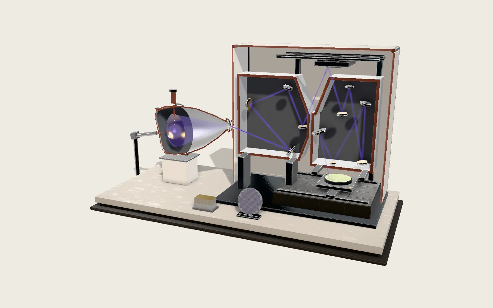 Plate F01EUV Lithography MachineLight 13.5 nm long prints a chip’s circuits on silicon, four times smaller than the mask. It comes from tin droplets turned to plasma, and travels only by mirrors.
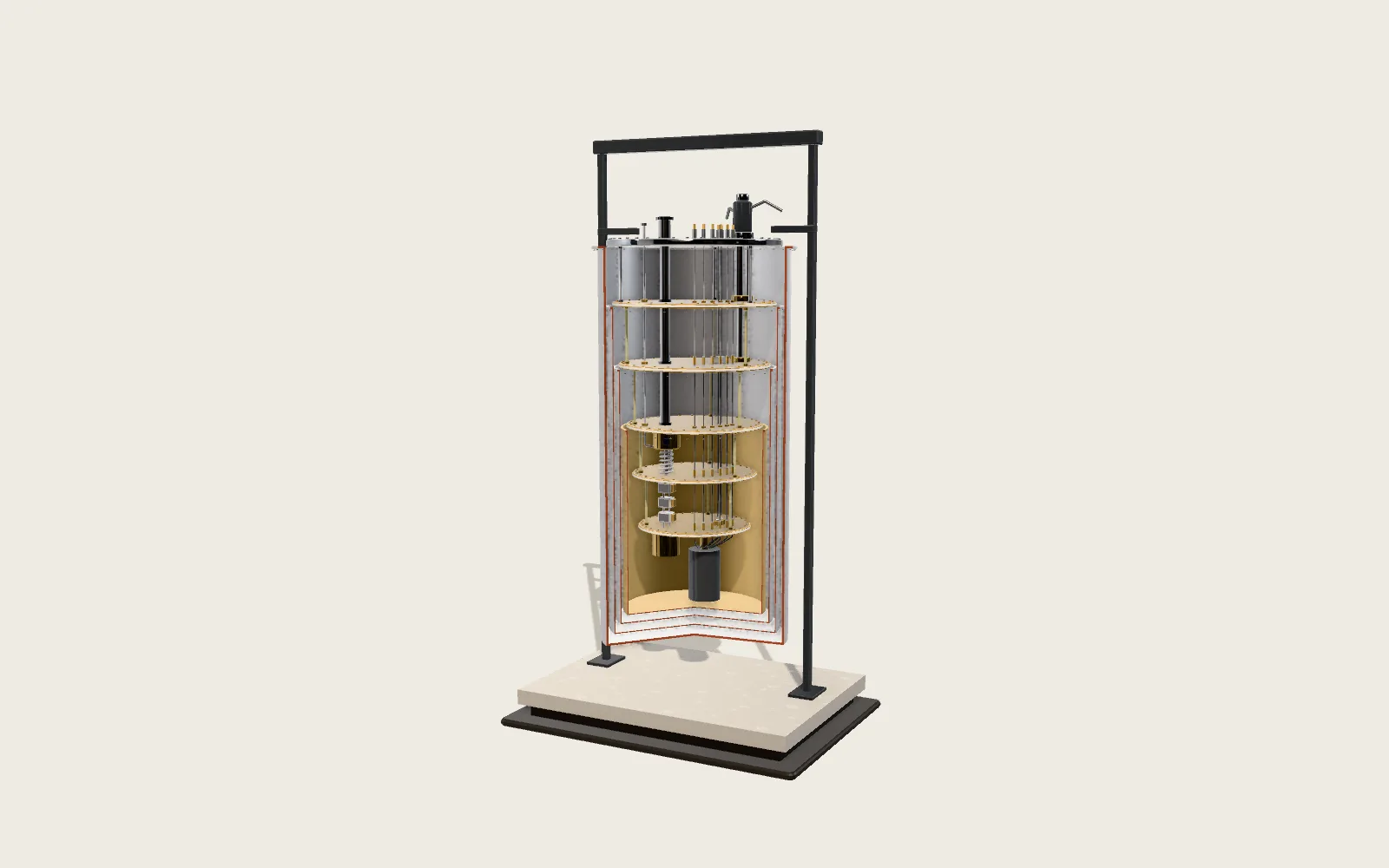 Plate F05The Dilution RefrigeratorA superconducting quantum computer hangs from a gold-plated “chandelier”. Each stage is colder than the one above; the last is about 10 mK, hundreds of times colder than space.