The TPU and Its Systolic Array
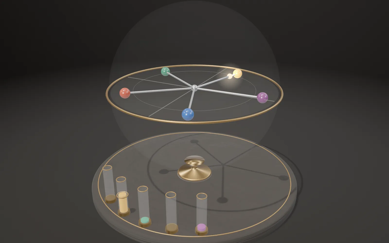
Weights stay put, inputs flow in from the left, sums flow down: a number read once is used many times.
Chapters · 14
Scroll
What It Does
The first TPU is a chip Google designed itself; from 2015 it ran the inference of neural networks in Google’s datacenters, working out answers with networks already trained. Its heart is a 256 × 256 matrix multiply unit: 65,536 8-bit integer multiply–accumulators, up to 92 trillion operations a second.
The 2017 paper compared it with the Intel Haswell CPU and the NVIDIA K80 GPU in the same datacenters, on six of Google’s own inference applications. By the paper’s weighted means it was about 15 times as fast as the K80 and about 30 times as fast as Haswell; leaving out the host server’s power, its performance per watt was about 29 times the K80’s and 83 times Haswell’s.
On the stand, left: the first TPU’s card. Right: its matrix multiply unit enlarged, an 8 × 8 systolic array; the real one has 256 × 256 cells. The blue tiles are inputs, the red ones partial sums, the brass plates weights.
First TPU: 65,536 8-bit MACs · 92 trillion operations a second · about 15 times its GPU, 30 times its CPU
Networks Multiply Matrices
A layer of a neural network is a set of “neurons”: each multiplies the previous layer’s outputs by its own weights, adds them up and passes the sum through a nonlinear function, such as turning negatives into 0. All of a layer’s multiply–adds together are one matrix multiply: a vector of inputs times a matrix of weights.
A batch of inputs makes it a matrix times a matrix. In fully connected layers, convolutions and the gates of an LSTM, these multiply–adds take the most time; the nonlinear functions and pooling run on the TPU in circuits outside the matrix unit.
The paper lists what the TPUs deployed in July 2016 were running: multilayer perceptrons about 61 %, LSTMs about 29 %, convolutional networks about 5 %. Its six chosen applications stand for 95 % of the TPUs’ workload.
TPUs deployed in July 2016: multilayer perceptrons 61 % · LSTMs 29 % · CNNs 5 %
One Multiply–Accumulate Cell
Each cell of the array does one thing: it multiplies the input x flowing in by the weight w it holds and adds the product to the partial sum s from the cell above; then it passes x on to the cell on its right and the new sum to the cell below.
The first TPU multiplies 8-bit integers: the products are 16 bits, the sums 32. The figures the paper cites: an 8-bit integer multiply takes about a sixth of the energy and a sixth of the area of a 16-bit floating-point multiply.
Training uses floating point. Before inference the weights are turned into 8-bit integers, a step called quantization; for inference, the paper says, that is usually good enough.
One cell: s ← s + x · w · 8 bits × 8 bits → 16 bits · summed in 32 bits
The Systolic Array
The paper’s Figure 4: the weights are loaded from the top and then stay put; data flows in from the left; partial sums move down. At every clock each number moves one cell on. The structure is called a systolic array, after the heart’s systole: data pulses through the cells in step with the clock.
The inputs go in skewed: the second row a clock after the first, the third a clock later again. So one multiply–accumulate sweeps through the array as a diagonal wavefront from the top left to the bottom right, and each column hands a finished sum out at its foot, into an accumulator.
To software it looks as if 256 inputs were read at once and updated 256 accumulators at once. On the stand, an 8 × 8 version, slowed to over half a second a clock.
Weights loaded from the top · data in from the left · partial sums down · one cell a clock
Read Once, Use Many Times
The paper: reading a large SRAM takes much more power than arithmetic, so the matrix unit runs systolically to cut reads and writes of the Unified Buffer.
In a 256 × 256 array an input read once is used 256 times along its row; a tile of weights loaded once is used once for every row of inputs in the batch. Without the cell-to-cell passing, every multiply–add would fetch two numbers.
For the batch of 200 rows the paper’s MLP0 used: one fetch per operand would take about 26.2 million numbers, the systolic array reads about 117 thousand, some 225 times fewer. This page computes that from a model.
256 × 256, a batch of 200 rows: about 26.2 million fetches one by one · about 117 thousand reads systolically
The Package Cut Open
In the paper’s photograph the first TPU sits on a card that fits the slot for a SATA disk in a server, linked to the host by PCIe Gen3 x16. The silver square in the middle is the package’s lid; the heat sink presses on it.
On the stand a corner of the lid is cut away: under it is the die, with thermal paste between die and lid. The die is made in a 28 nm process, clocked at 700 MHz, with a thermal design power of 75 W and about 40 W measured when busy. The paper gives no number for its area, only that it is under half the Haswell die’s (662 mm²).
Under the cut corner lies the die’s upper right block: the matrix multiply unit. The card’s, the lid’s and the die’s sizes are estimates from the paper’s photograph.
28 nm · 700 MHz · 75 W design power, about 40 W busy · die under 331 mm²
The Floor Plan
The paper’s Figure 2 is the die’s floor plan. The 24 MiB Unified Buffer holds the intermediate results and takes about 29 %; the matrix multiply unit about 24 %. Together they are nearly two thirds of the die.
Below them: the 4 MiB of accumulators (6 %), the activation pipeline (6 %), the host interface and PCIe, with the DRAM ports at both sides. Control is just 2 %; in CPUs and GPUs, the paper notes, control is much larger and much harder to design.
On the stand the lid is lifted and the blocks shaded in the paper’s colours: blue holds data, yellow computes, green is input and output, red is control. The 2018 CACM version gives the matrix unit 29 %; this page uses the ISCA paper’s figure.
Unified Buffer 29 % · matrix unit 24 % · accumulators 6 % · activation 6 % · control 2 %
Waiting for Weights
The weights live off the chip in 8 GiB of DDR3, the paper’s Weight Memory: the two rows of small black chips above and below the package. It delivers just 34 GB a second.
They enter the array through a Weight FIFO four tiles deep. A tile is 256 × 256 8-bit numbers, 64 KiB, and takes 256 clocks to shift in; the array holds two, one computing while the next loads.
To keep the array busy, each byte of weights read must serve about 1,350 multiply–adds. The multilayer perceptrons and LSTMs manage only 64 to 200, so four of the six applications are limited by memory bandwidth, and on average the matrix unit waits for weights in 43 % of the clocks. With GDDR5 memory like the K80’s, the paper’s performance model estimates, it would compute about three times as fast.
Weight Memory: 8 GiB DDR3 · 34 GB a second · balance point: about 1,350 multiply–adds per weight byte
Training Needs Floating Point
The first TPU did inference only; Google trained on GPUs it bought. Training needs backpropagation, numbers of wider range, more memory, and many chips working together. The second TPU, of 2017, was designed for it: two cores to a chip, each with one 128 × 128 matrix unit that multiplies in bfloat16 and adds in 32-bit floating point.
bfloat16 is a 16-bit floating-point format: 1 sign bit, 8 exponent bits, 7 mantissa bits. Its exponent is as wide as 32-bit floating point’s, so it spans the same range, with fewer significant digits.
Data moved into HBM beside the die (16 GiB at 700 GB a second on the second TPU), and dedicated links joined the chips into pods of 256. The third TPU, of 2018, has four matrix units to a chip, 123 trillion bfloat16 operations a second, liquid cooling, and pods of 1,024.
bfloat16: 1 sign bit · 8 exponent bits · 7 mantissa bits · multiply in bfloat16, add in 32 bits
4,096 Chips
TPU v4 went into service in 2020: two cores to a chip, each with four 128 × 128 matrix units, 275 trillion bfloat16 operations a second; in the package beside the die, four HBM stacks hold 32 GiB at 1,200 GB a second.
Sixty-four chips are wired as a 4 × 4 × 4 cube, and 64 cubes are joined through 48 optical circuit switches into one machine of 4,096 chips. Inside a switch, MEMS mirrors turn to send a fibre’s light on to another cube; the light is not turned into electricity there. The paper says the switches and optics are under 5 % of the machine’s cost and under 3 % of its power.
Later pods grew: in Ironwood, of 2025, each chip has four 256 × 256 matrix units and a pod holds 9,216 chips. Its 4,614 trillion operations a second per chip are 8-bit floating point; in bfloat16 it is 2,307 trillion.
TPU v4: 4,096 chips · 64 cubes of 4 × 4 × 4 · 48 optical circuit switches
Against Their Contemporaries
The first TPU was compared with the Haswell CPU and the K80 GPU in the same datacenters in 2015, on Google’s six inference applications: about 15 times (against the GPU) and about 30 times (against the CPU) are weighted means that include the host’s overhead. App by app, the gain ran from none over the K80 (LSTM1) to 71 times the CPU (CNN1).
The TPU v4 paper: on systems of about 32 chips running Google’s applications, 2.1 times TPU v3’s speed and 2.7 times its performance per watt. Against NVIDIA’s A100 it uses published MLPerf Training 2.0 results with about 4,096 chips on each side: 1.15 times as fast on BERT, 1.67 times on ResNet; on systems of 64 chips, the A100 drew 1.3 to 1.9 times the power.
Each ratio sets one generation against chips of its own time, on given applications at a given scale; held up against today’s GPUs, it says nothing.
First TPU vs K80, Haswell: about 15, 30 times · v4 vs v3: 2.1 times · v4 vs A100: 1.15–1.67 times
What It Does Not Say
A TPU is not fast at everything. It is built for dense matrix multiplies; when the matrices are too small to fill the array, or the weights have not arrived, it idles. On the six applications the first TPU did matrix work in only 28 % of its clocks on average, and its useful multiply–adds came to 23 % of peak: 21.4 trillion operations a second on average, not 92.
Google’s documentation lists programs that suit TPUs badly: those with frequent branching, with many element-wise operations, needing high-precision arithmetic, or with custom operations in the training loop. It has none of the caches or out-of-order execution of general-purpose processors; their absence, the paper says, helps explain why, with so many multipliers and so much memory, it is relatively small and low-power.
Nor did Google invent the systolic array: H. T. Kung and Charles Leiserson proposed it at Carnegie-Mellon University in 1978.
First TPU, mean of six applications: matrix unit busy 28 % · useful multiply–adds 23 % · 21.4 trillion a second
Taken Apart
The stand comes apart: the card, its weight memory, the package substrate, the die and the lid; at the right, the array’s cells, the weight FIFO behind them and the accumulators in front.
The thermal paste stays on the lid’s underside; lift it and the die’s floor plan shows. Every cell of the array is one multiply–accumulate unit.
The card’s and the die’s sizes are estimates from the photograph; heights off the board are drawn ×1.5.
Card · weight memory · substrate · die · lid · multiply–accumulate cells · weight FIFO · accumulators
Laboratory
The lever sets how many rows a batch of inputs has, from 1 to 32; the weights can fill the array (8 × 8) or part of it (8 × 4, 4 × 4). Run: the weights shift into the array row by row from the back, then the inputs flow through, one matrix multiply.
The readouts count for this 8 × 8 model: the clocks for loading the weights and for computing, the multiply–adds done, the share of cell-clocks spent on useful multiply–adds, and the numbers read from memory against the fetches one multiply–add at a time would need.
The larger the batch, the less the clocks spent filling and draining the array show. It is a model: the real matrix unit is 256 × 256, and the paper says its matrix instructions are pipelined one after another, so the next instruction can cover those clocks.
Readouts: clocks · multiply–adds · utilisation · numbers read
Try thisWith a batch of one input row, how much of its time does the 8 × 8 array spend waiting? With a batch of 32? And when the weights fill only half the columns?
What the model leaves out
The card and the die follow the paper’s photograph and floor plan, but the paper gives no dimensions: the card’s size, the parts’ sizes and the die’s sides are estimates, heights off the board are drawn ×1.5, and the die is drawn at the floor plan’s aspect with the paper’s upper bound on its area. The lid is cut only to show the die. The array is an 8 × 8 version of the 256 × 256 one, slowed to over half a second a clock; the numbers’ sizes are not drawn: a red sum grows one step with each product added, and each step in an accumulator is one row of results. In the real array the weights shift in as whole tiles and data and control are pipelined; this page counts the clocks of one multiply on its own, without that overlap.
Easy to get wrong
A TPU is not faster than a GPU at everything: every ratio has conditions, compares chips of the same years, and uses Google’s own applications. The first TPU did inference, not training. Google did not invent the systolic array. Its “92 trillion operations a second” are 8-bit integer operations, not floating-point ones; the balance point of 1,350 counts multiply–adds, while the 92 trillion count each multiply–add as two operations. The 61 %, 29 % and 5 % are shares of the deployed TPUs by type of application, not shares of the arithmetic. Ironwood’s 4,614 trillion are 8-bit floating point. The optical switches only redirect fibres; the chips do not compute with light.
Common questions · 5
- What is a TPU?
The first TPU is a chip Google designed itself; from 2015 it ran the inference of neural networks in Google’s datacenters, working out answers with networks already trained.
01What It Does ↑- What is a systolic array?
The paper’s Figure 4: the weights are loaded from the top and then stay put; data flows in from the left; partial sums move down.
04The Systolic Array ↑- Why does the TPU use a systolic array?
The paper: reading a large SRAM takes much more power than arithmetic, so the matrix unit runs systolically to cut reads and writes of the Unified Buffer.
05Read Once, Use Many Times ↑- What is bfloat16?
bfloat16 is a 16-bit floating-point format: 1 sign bit, 8 exponent bits, 7 mantissa bits.
09Training Needs Floating Point ↑- Is a TPU faster than a GPU at everything?
A TPU is not fast at everything.
12What It Does Not Say ↑
Sources
- Jouppi et al. (2017): In-Datacenter Performance Analysis of a Tensor Processing Unit, ISCA 2017
- Jouppi, Young, Patil, Patterson (2018): A Domain-Specific Architecture for Deep Neural Networks, Communications of the ACM 61(9)
- Sato, Young, Patterson (2017): An in-depth look at Google’s first Tensor Processing Unit (TPU), Google Cloud blog
- H. T. Kung, Charles E. Leiserson (1978): Systolic Arrays (for VLSI), Carnegie-Mellon University report CMU-CS-79-103
- H. T. Kung (1982): Why Systolic Architectures?, IEEE Computer 15(1)
- Norrie et al. (2020): Google’s Training Chips Revealed: TPUv2 and TPUv3, Hot Chips 32 talk
- Wang, Kanwar (2019): BFloat16: The secret to high performance on Cloud TPUs, Google Cloud blog
- Jouppi et al. (2023): TPU v4: An Optically Reconfigurable Supercomputer for Machine Learning with Hardware Support for Embeddings, ISCA 2023
- Jouppi, Lakshmanamurthy, Young, Patterson (2026): Google’s Training Supercomputers from TPU v2 to Ironwood, IEEE Micro (preprint)
- Google Cloud documentation: TPU architecture
- Google Cloud documentation: Introduction to Cloud TPU
- Google Cloud documentation: TPU7x (Ironwood)
- Vahdat (2025): Ironwood: The first Google TPU for the age of inference, Google blog
Data
The card follows the photograph of the first TPU’s printed circuit board and the die its floor plan, both in Jouppi et al., “In-Datacenter Performance Analysis of a Tensor Processing Unit” (ISCA 2017), redrawn. The paper gives no dimensions: the card’s size and every part’s are estimates from the photograph, heights are drawn ×1.5, and the die is drawn at the floor plan’s aspect with the paper’s upper bound on its area. The cut through the lid is a drawing choice. The 8 × 8 array, its tokens and the laboratory’s counts are a model of a weight-stationary systolic array (the real matrix unit is 256 × 256), computed by this page (src/topics/tpu/systolic.js, docs/plates/tpu/computed-v1.py). Material presets, parts and the softbox studio of the site’s model kit are ported from AirsupHQ/machine-skill (MIT, © 2026 Air Supply Technologies Inc.).
The text, pictures and models on this page are licensed CC BY-NC 4.0: free to use and adapt for teaching and other non-commercial purposes, with credit to world.lapla.si. Third-party material listed above keeps its own licence.
Cite this plate
Laplace’s Mini World, Plate F53, “The TPU and Its Systolic Array”, https://world.lapla.si/en/tpu/, CC BY-NC 4.0, updated 2026-10-27.
Follow the question
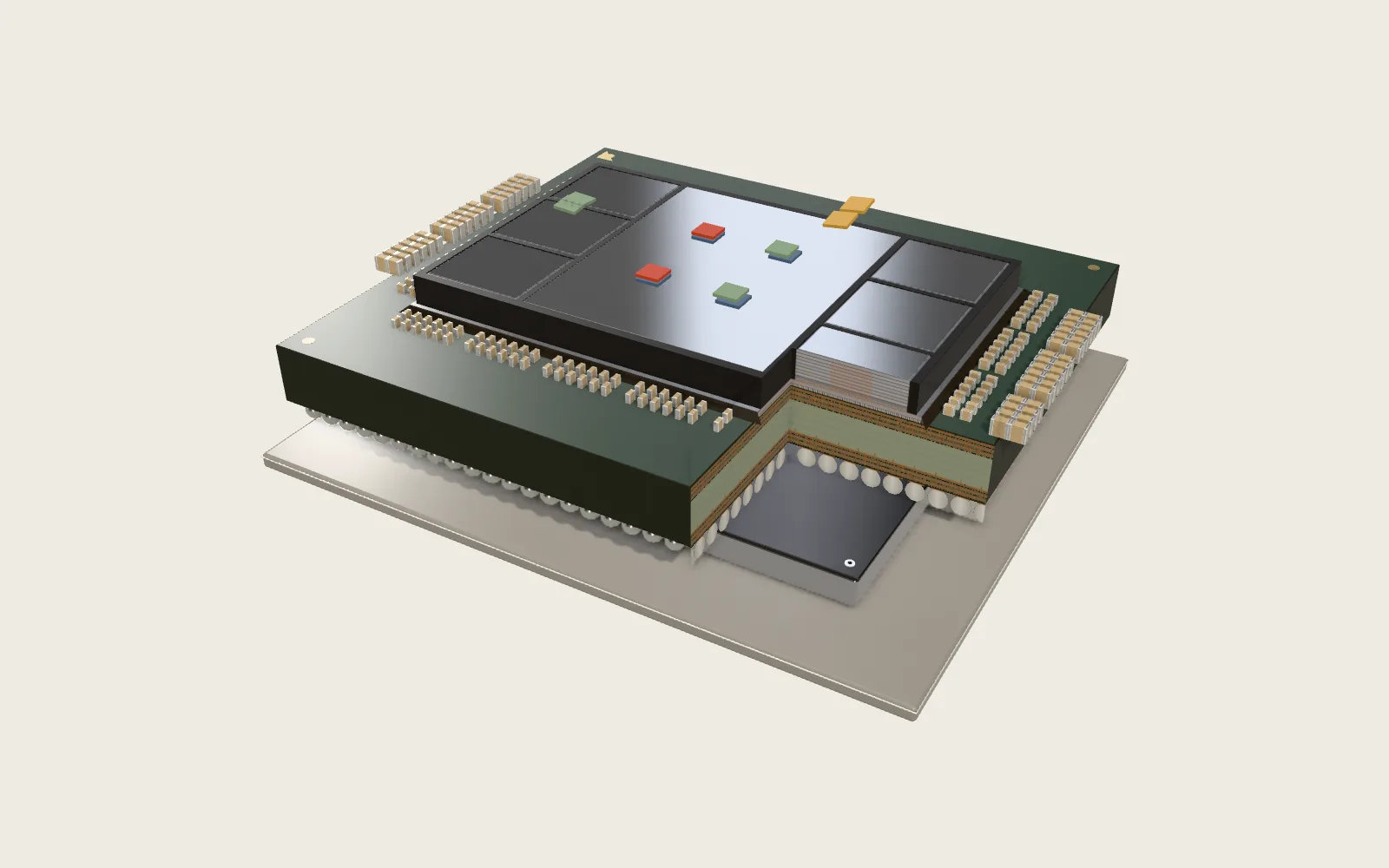 Plate F51FlashAttention and GPU MemoryDone the standard way, attention in a Transformer is slow on a GPU less because of its arithmetic than because an N × N matrix of scores is written to memory and read back. FlashAttention cuts the work into blocks, finishes each in the chip’s shared memory and keeps a running softmax, so it gets the same result while that matrix never goes to memory.
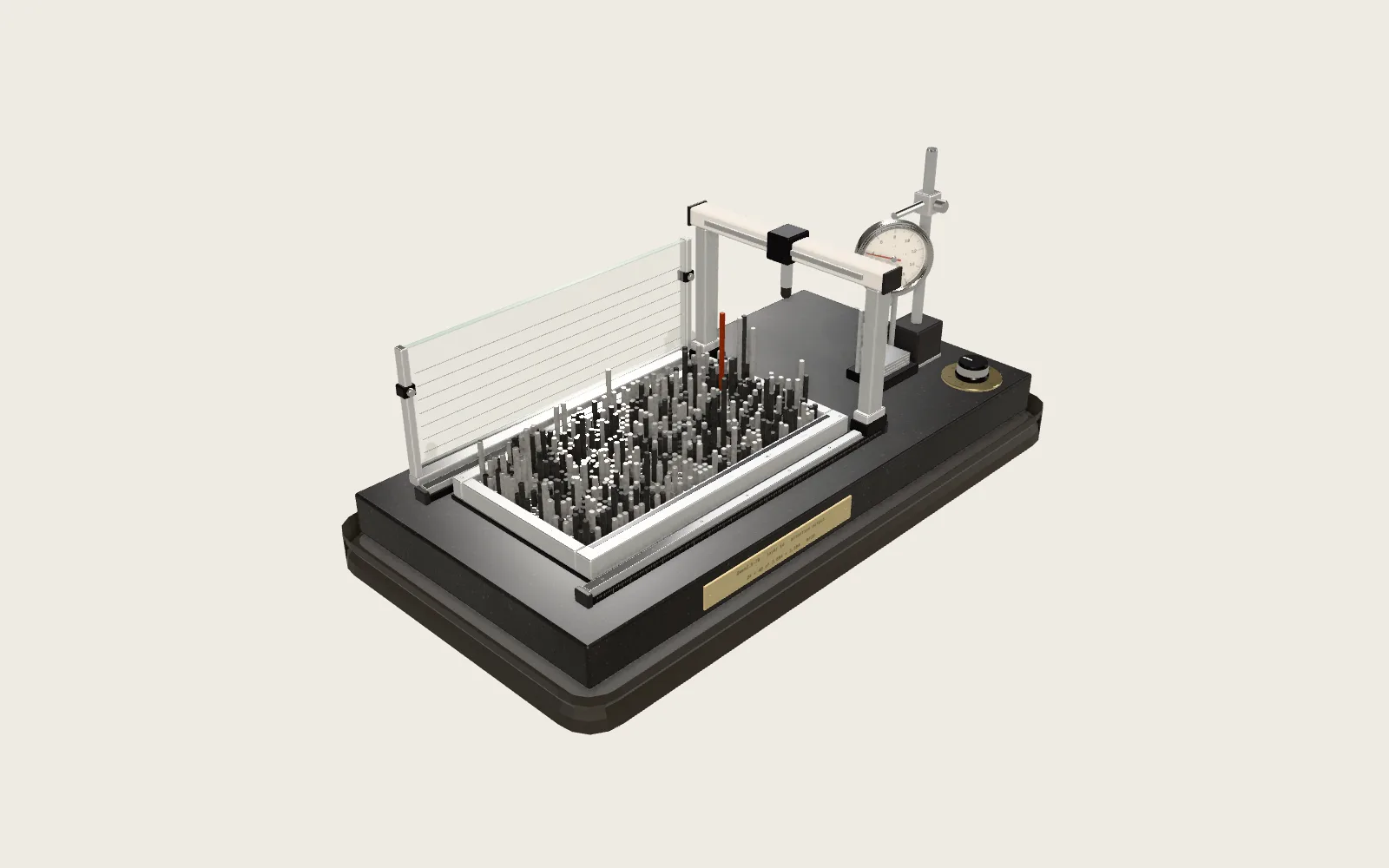 Plate F43LLM QuantizationA language model’s weights are stored with 16 bits each. Quantizing rounds them onto a coarser grid: 8 bits, 4, or only −1, 0 and +1. The model gets several times smaller and faster to read, at a cost in accuracy.
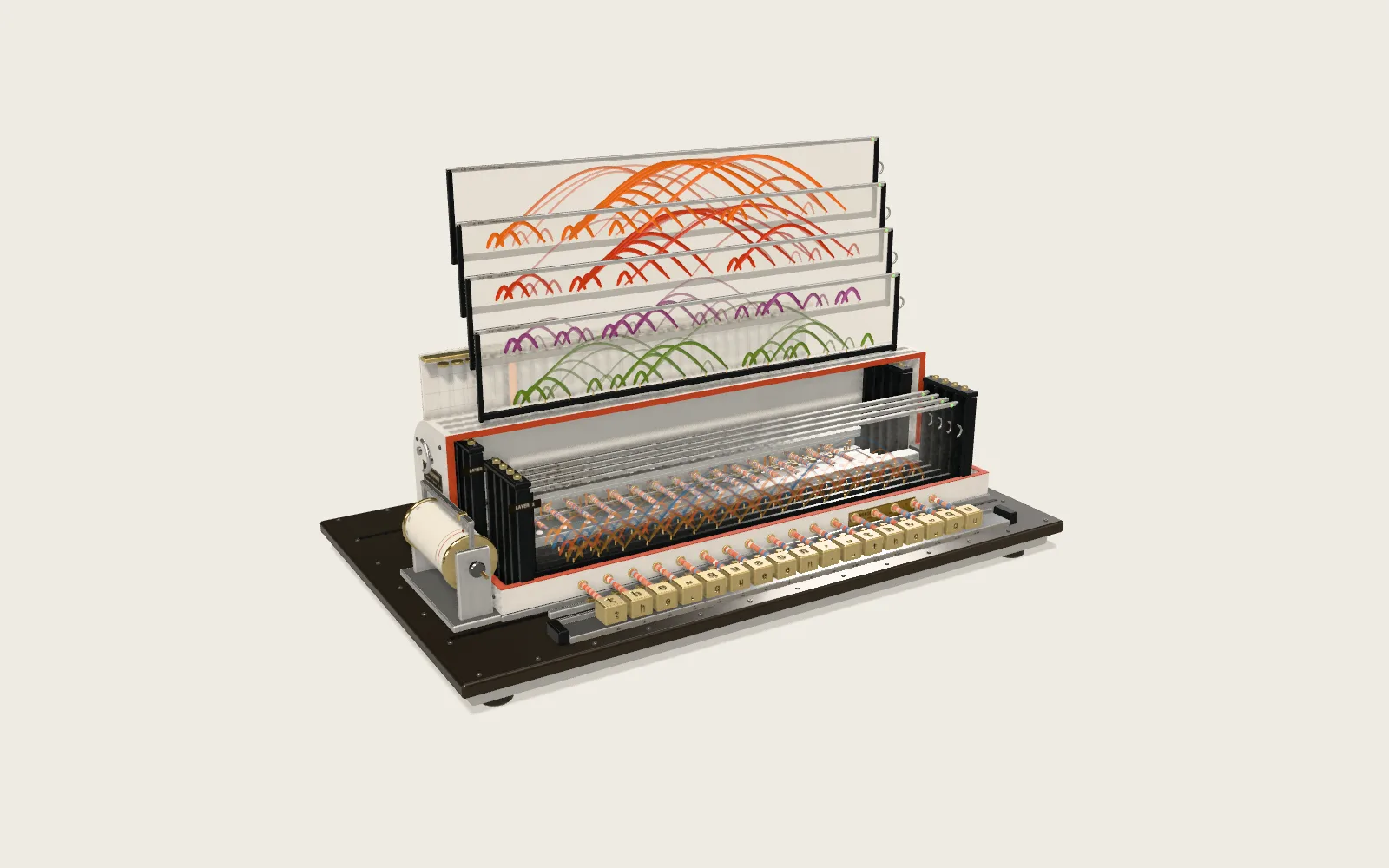 Plate F13Attention in TransformersA two-layer, eight-head Transformer reads a sentence in your browser, one character at a time, and guesses the next. Each thread is one act of attention; its brightness is the weight.
 Plate F25The Mixture of ExpertsA model can hold hundreds of billions of parameters and use only a small share of them on each word: a router picks a few “experts” for it and the rest stay idle. Here is a small trained one, with 16 experts and 2 per letter.