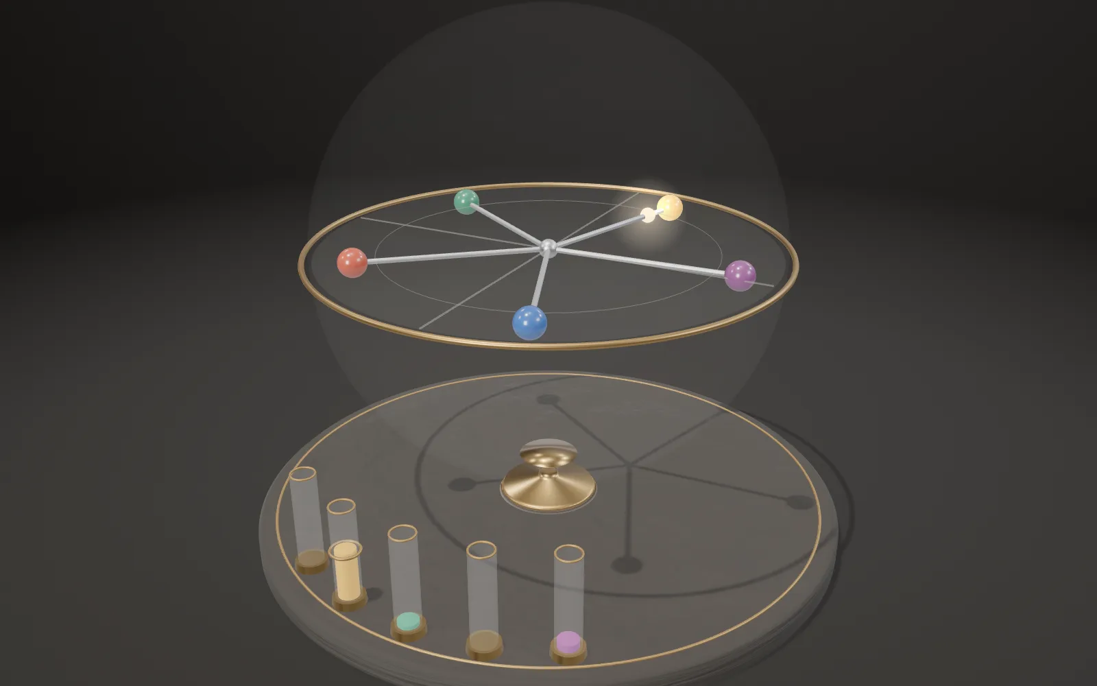
FlashAttention and GPU Memory
Attention’s N × N matrix never has to go to memory.
Chapters · 14
- 01What it does
- 02Where the data lives
- 03Fast to compute, slow to move
- 04The standard way: a round trip
- 05The package cut open
- 06Inside the die
- 07Blocks
- 08A softmax with a running tally
- 09Backward: recomputing beats reading
- 10How much faster, how much less memory
- 11The second and third versions
- 12What it does not claim
- 13Taken apart
- 14Laboratory
Scroll
What it does
Attention in each layer of a Transformer compares every position in a sequence with every position: N positions make an N × N matrix of scores. The standard way writes that matrix to the GPU’s memory (HBM) and reads it back for the softmax. FlashAttention, published in 2022, computes the same attention, not an approximation, and that matrix never goes to memory.
The paper measured GPT-2 medium’s attention on an A100 GPU (sequence length 1,024, batch 64, forward and backward): data read from and written to memory fell from 40.3 GB to 4.4 GB and the time from 41.7 to 7.3 ms, while the arithmetic grew by about 13 %. The memory it needs grows linearly with sequence length, not with its square.
Two later versions are faster. The second (2023) reached up to 225 trillion floating-point operations a second per A100 when training GPT-style models; the third (2024) runs the forward pass 1.5 to 2.0 times faster again on an H100. On the stand is a model of a GPU package laid out like NVIDIA’s H100 SXM5: the die in the middle, memory stacks on either side, and coloured tiles for the data moving between them.
GPT-2 medium, A100: memory traffic 40.3 → 4.4 GB · 41.7 → 7.3 ms · about 13 % more arithmetic
Where the data lives
A GPU’s memory comes in levels: the larger, the slower. On an H100 SXM5 the HBM beside the die holds 80 GB and delivers 3.35 TB a second; the L2 cache on the die holds 50 MB; further in, each of the 132 streaming multiprocessors (SMs) has up to 228 KB of shared memory and 256 KB of registers.
All 132 SMs’ shared memory adds up to about 30 MB, more than two thousand times less than the HBM, but it sits next to the units that compute. The FlashAttention-3 paper estimates its total bandwidth at about 31 TB a second and the L2’s at about 12 TB a second, several times the HBM’s.
The papers’ “SRAM” is this shared memory and the registers, not the L2. On the stand, the six blocks beside the die are the HBM sites: NVIDIA lists 5 HBM3 stacks of 16 GB for H100 SXM5 and does not say what the sixth site holds. The large block in the middle is the GH100 die, 814 mm².
HBM 80 GB · 3.35 TB/s → L2 50 MB → per SM: 228 KB shared memory · 256 KB registers
Fast to compute, slow to move
Whether an operation is fast depends on how much arithmetic it does for each byte it moves. The tensor cores of an H100 SXM5 do up to 989 trillion 16-bit floating-point operations a second, while its memory delivers 3.35 TB a second: to keep the chip busy, each byte has to feed about 295 operations.
A matrix multiplication uses each number it reads many times and gets there. Elementwise operations and reductions do not: softmax, dropout and masking read each number once, do a little with it and write it back, and their time goes into moving data. The FlashAttention paper calls them memory-bound.
Counted the standard way (16-bit, one attention head, head dimension d = 128), the whole of attention does about 62 operations per byte moved, nearly five times short of 295. The softmax step alone, roughly estimated, does about one.
H100 SXM5: 989 trillion/s ÷ 3.35 TB/s ≈ 295 operations per byte · standard attention (d = 128): about 62
The standard way: a round trip
The standard way takes three steps. Read Q and K from memory, compute the scores S = QKᵀ, write S back. Read S, compute P = softmax(S), write P back. Read P and V, compute O = PV, write O back.
With a sequence of N = 4,096 and a head dimension of d = 128, one head’s S is 4,096 × 4,096 16-bit numbers, 33.6 MB, 32 times the size of Q. Writing and reading S and P once each moves 134 MB, about 40 microseconds at 3.35 TB a second; the same head’s two matrix multiplications take about 8.7 microseconds at peak.
In training, P must also be kept for the backward pass and read again. The stand plays it at a small scale, 8 × 8 blocks: the red blocks of scores fly into memory and back, twice.
N = 4,096, d = 128, one head: S 33.6 MB · S and P out and back 134 MB ≈ 40 µs · matrix multiplications ≈ 8.7 µs
The package cut open
The memory is not in the die but in stacks beside it. Each HBM stack is several DRAM dies piled up and joined by through-silicon vias (TSVs). JEDEC’s HBM3 standard defines stacks 4, 8 and 12 high, with 8 to 32 Gb per layer. An H100 stack holds 16 GB, which with 16 Gb layers is 8 of them; NVIDIA does not state it, and the model draws 8.
Each stack connects to the die by 1,024 data lines. The 5 stacks of an H100 SXM5 make 5,120 bits; at about 5.24 Gb a second per line that is 3,352 GB a second, about 670 GB a second per stack.
In packages like TSMC’s CoWoS-S, a logic die and its HBM sit side by side on a large silicon interposer, wired together through it, above the package substrate and its solder balls. NVIDIA does not publish the layers or sizes of the H100 package; the model draws them after this kind of package, with thicknesses ×4.
HBM3: 1,024 bits per stack · H100 SXM5: 5 stacks, 5,120 bits · 3,352 GB a second
Inside the die
The GH100 die is made on TSMC’s 4N process: 80 billion transistors on 814 mm². The full die has 8 graphics processing clusters (GPCs) with 144 SMs in all; an H100 SXM5 enables 132 of them. In the middle is the 50 MB L2 cache (60 MB on the full die), and along the sides the memory controllers for the stacks.
Each SM has 4 tensor cores, built for multiplying small blocks of matrices; four register files of 64 KB, 256 KB in all; and 256 KB of L1 cache and shared memory, of which up to 228 KB can be shared memory. This is where FlashAttention keeps its blocks.
The white plaque rising over the die is NVIDIA’s block diagram of GH100, drawn at the size of the die. It shows what the chip is made of, not where the parts lie on it.
GH100: 814 mm² · 144 SMs, 132 used on H100 SXM5 · per SM: 4 tensor cores, 228 KB shared memory, 256 KB registers
Blocks
FlashAttention never computes S whole. It cuts Q into blocks of B_r rows and K and V into blocks of B_c rows, reads one block of Q and one block each of K and V into an SM’s shared memory, computes that small block of scores on the chip and uses it at once.
The first paper sets the block sizes from the shared memory’s size M: B_c = ⌈M / 4d⌉, B_r = min(⌈M / 4d⌉, d). It proves that the standard way needs Θ(Nd + N²) reads and writes of memory and FlashAttention Θ(N²d²/M): when d² is much smaller than M, many times fewer. Real kernels pick block sizes by hand for each head dimension; the second paper gives {64, 128} × {64, 128}.
The whole computation is fused into one GPU program: load, multiply, softmax, mask, dropout, multiply, and only the output O is written back. On the stand, in the second version’s order, each SM takes one block of Q at a time; blocks of K and V fly in, the red block of scores lights on the chip and is gone, and the finished block of O flies back.
Blocks: B_r rows of Q, B_c rows of K and V · memory traffic: standard Θ(Nd + N²), FlashAttention Θ(N²d²/M)
A softmax with a running tally
A softmax needs a row’s maximum and the sum of its exponentials before it can turn scores into weights. Once the work is cut into blocks, only part of a row is in view at a time. The way out is to keep two running numbers: the largest score so far, m, and the sum of exponentials measured from it, ℓ.
Each new block brings its own maximum. If that is larger than m, the sum so far and the output so far are multiplied by e^(m_old − m_new) to move them to the new reference, and the block is added in. After the last block the result is the same as a softmax over the whole row, up to rounding: not an approximation. This online softmax was used in 2018 to cut a softmax’s memory traffic, and in 2021 to cut the memory attention takes.
The figure runs a row of 8 scores, 2 at a time: after four steps m is 3.4 and ℓ is 2.170462, and the output differs from the direct one by less than 10⁻¹⁵.
m_new = max(m, m̃) · ℓ_new = e^(m − m_new)·ℓ + e^(m̃ − m_new)·ℓ̃ · the same as a softmax over the whole row
Backward: recomputing beats reading
Training also runs backward, and the backward pass needs S and P. The standard way keeps P in memory and reads it then. FlashAttention keeps only the output O and two numbers per row (m and ℓ), and rebuilds S and P block by block from Q, K and V. It does not keep the dropout mask either, only the random-number generator’s state, and makes the mask again.
That adds arithmetic and removes traffic. On an A100, for GPT-2 medium’s attention (sequence 1,024, head dimension 64, 16 heads, batch 64, forward and backward), the paper measured about 13 % more operations, memory traffic down from 40.3 GB to 4.4 GB, about 9 times less, and the time down from 41.7 ms to 7.3 ms, about 5.7 times faster.
So the extra memory it needs grows only linearly with N: a few numbers per row.
GPT-2 medium, A100, forward + backward: about 13 % more operations · memory traffic 40.3 → 4.4 GB · 41.7 → 7.3 ms
How much faster, how much less memory
The memory saving is the plainest. On a 40 GB A100 (batch 16, 8 heads, head dimension 64), at a sequence of 4,096 PyTorch’s standard attention used 17,024 MB and FlashAttention 836 MB, about 20 times less. For longer sequences the paper’s table has no figure for the standard way; FlashAttention reaches 65,536 with 13,376 MB.
Training got faster too: BERT-large (sequence 512) on 8 A100s trained 15 % faster than the MLPerf 1.1 record; GPT-2 (sequence 1K) about 3 times faster than the HuggingFace implementation and about 1.7 times faster than Megatron-LM. Each speed-up has its own baseline.
Longer sequences became trainable as well: on Path-X (sequences of 16K) a Transformer with FlashAttention was the first to do better than chance, 61.4 %; the longer Path-256 (64K) used the approximate block-sparse version, 63.1 %.
A100 40 GB, N = 4,096: 17,024 → 836 MB · BERT-large 15 % faster · GPT-2 about 3 times faster than HuggingFace
The second and third versions
The first version used only 25–40 % of an A100’s peak. The second (2023) changed three things: fewer operations outside the matrix multiplications, since an A100’s tensor cores do 312 trillion 16-bit matrix operations a second but its ordinary 32-bit units only 19.5 trillion, so each non-matrix operation costs 16 times as much; even a single head’s work split along the sequence across thread blocks, to keep more SMs busy; and a different division of work inside each thread block, with less exchange between warps through shared memory. It is about twice as fast as the first, at 50–73 % of the A100’s peak.
On an H100 the same code reaches about 35 %. The third version (2024) was rebuilt for it. A dedicated copy unit (the TMA) moves blocks into shared memory asynchronously, while some warps only move data and others only compute. The exponentials are staggered too: an H100 does 989 trillion matrix operations a second but only 3.9 trillion special functions such as exponentials, so one group of warps does its softmax while another multiplies.
The result: forward passes 1.5–2.0 times faster than the second version, up to 740 trillion 16-bit operations a second, 75 % of the 989 trillion peak (840 trillion and 85 % in the version published at NeurIPS 2024; both at head dimension 256 and long sequences); with 8-bit floats, close to 1,200 trillion (1,300 trillion in the published version).
Second version: 50–73 % of an A100’s peak · third version, H100, forward: 740 trillion/s (75 %), published 840 (85 %)
What it does not claim
FlashAttention computes the original attention, not an approximation: results differ only by floating-point rounding, and in 16-bit the error is smaller than the standard implementation’s, because the softmax’s intermediate values are kept in 32-bit. The approximate method in the paper is a separate one, block-sparse FlashAttention.
It does not reduce the arithmetic: the same in the forward pass, somewhat more in the backward pass because of recomputation, and still growing with the square of N. What it reduces is memory traffic and the memory used. Q, K, V and O still go in and out of memory, and K and V are read several times.
How much faster depends on the conditions: the GPU’s memory bandwidth and shared-memory size, the head dimension, the sequence length, and whether there is masking or dropout all change it; at head dimension 128 the blocks get smaller and the gain shrinks. Each variant of attention needs a new low-level GPU program, and a new GPU generation may need it rewritten. On TPUs, a related method saw no speed-up: there compute and bandwidth were already balanced.
Exact, not approximate · no less arithmetic, still growing with N² · the gain depends on the GPU, head dimension and sequence length
Taken apart
The stand comes apart in five pieces: the HBM stacks, the GH100 die, the silicon interposer with the moulding that fills the gaps, the package substrate with its capacitors and solder balls, and the display base.
Of the six stack sites, an H100 SXM5 uses five, and NVIDIA does not say what the sixth is; the cut one shows eight DRAM layers and the vias through them.
The small blocks on the substrate are capacitors; the cut face shows the substrate’s copper layers, its vias and the solder balls beneath. Every thickness is drawn ×4.
HBM stacks · die · interposer and moulding · package substrate · display base
Laboratory
The lever sets the sequence length N, from 512 to 65,536; the head dimension d and the block size can be chosen. The readouts count memory reads and writes for the two algorithms (16-bit, one head, forward). The standard way reads and writes Q, K, V and O once each and writes and reads S and P once each. FlashAttention, in the second version’s order, reads each block of Q once, reads all of K and V once for every block of Q, and writes O once, with no help from the L2 cache counted.
Larger blocks mean fewer passes over K and V, but one block each of Q, K and V must fit in 228 KB of shared memory, and the block of scores and the output in 256 KB of registers. When they don’t, the readout says so.
The grid on the stand is the N × N matrix of scores, drawn in blocks; the lit block is the one an SM is computing. The standard way writes the whole grid to memory; FlashAttention writes none of it.
Readouts: the size of S · memory traffic (standard / FlashAttention) · shared memory and registers one block takes
Try thisDouble the sequence length: how many times more memory traffic does the standard way need, and FlashAttention? Change the head dimension from 64 to 128: does FlashAttention’s saving grow or shrink?
What the model leaves out
The model is not to scale. NVIDIA publishes only the die’s area, 814 mm²; the die’s sides and the sizes of the stacks, interposer and substrate are estimates, thicknesses are drawn ×4, and the solder balls are drawn larger and fewer. Data flies from five of the six stack sites, never from the cut one: NVIDIA says neither which site is unused nor what the sixth holds, and this one was chosen only for the drawing. The 8 DRAM layers follow from 16 GB per stack and 16 Gb per layer. The white plaque carries NVIDIA’s logical block diagram, not the chip’s physical layout. The flying tiles stand for blocks of the matrices: real data runs through wires in the interposer, not through the air, and there are far fewer blocks (8 × 8) and far slower flights than on a real chip. The laboratory’s “fits” is a rough model: real kernels also double-buffer, keep other values, and share an SM with other blocks.
Easy to get wrong
The papers’ “SRAM” is the SMs’ shared memory and registers, not the L2 cache. FlashAttention is not an approximation and does not reduce the arithmetic; it reduces memory traffic, and the online softmax it uses came before it. Watch the compute figures: the 1,979 trillion 16-bit operations a second on NVIDIA’s product page is “with sparsity”; dense is half, 989 trillion, and the utilization figures are shares of that. The first paper’s hardware figures (SRAM at 19 TB/s, 20 MB) are estimates for the A100, not the H100. Every speed-up has its own model, GPU, sequence length and baseline; none of them supports a general “N times faster”.
Common questions · 5
- Is FlashAttention an approximation?
FlashAttention computes the original attention, not an approximation: results differ only by floating-point rounding, and in 16-bit the error is smaller than the standard implementation’s, because the softmax’s intermediate values are kept in 32-bit.
12What it does not claim ↑- How many operations per byte keep an H100 busy?
The tensor cores of an H100 SXM5 do up to 989 trillion 16-bit floating-point operations a second, while its memory delivers 3.35 TB a second: to keep the chip busy, each byte has to feed about 295 operations.
03Fast to compute, slow to move ↑- Is a softmax computed in blocks the same as over the whole row?
After the last block the result is the same as a softmax over the whole row, up to rounding: not an approximation.
08A softmax with a running tally ↑- What does FlashAttention keep for the backward pass?
FlashAttention keeps only the output O and two numbers per row (m and ℓ), and rebuilds S and P block by block from Q, K and V.
09Backward: recomputing beats reading ↑- How much memory does FlashAttention save?
On a 40 GB A100 (batch 16, 8 heads, head dimension 64), at a sequence of 4,096 PyTorch’s standard attention used 17,024 MB and FlashAttention 836 MB, about 20 times less.
10How much faster, how much less memory ↑
Sources
- Dao, Fu, Ermon, Rudra, Ré (2022): FlashAttention: Fast and Memory-Efficient Exact Attention with IO-Awareness, NeurIPS 2022
- NeurIPS 2022 proceedings record (FlashAttention)
- Dao (2023): FlashAttention-2: Faster Attention with Better Parallelism and Work Partitioning, ICLR 2024
- Shah, Bikshandi, Zhang, Thakkar, Ramani, Dao (2024): FlashAttention-3: Fast and Accurate Attention with Asynchrony and Low-precision (arXiv version)
- FlashAttention-3, the NeurIPS 2024 version
- Milakov, Gimelshein (2018): Online normalizer calculation for softmax
- Rabe, Staats (2021): Self-attention Does Not Need O(n²) Memory
- The flash-attention repository (Dao-AILab, BSD 3-Clause)
- NVIDIA: NVIDIA H100 Tensor Core GPU Architecture whitepaper, V1.04
- NVIDIA: H100 product specifications (read 2026-10-26)
- NVIDIA Technical Blog (2022): NVIDIA Hopper Architecture In-Depth
- NVIDIA: Hopper Tuning Guide
- NVIDIA: CUDA C++ Programming Guide 12.6 (compute capability 9.0)
- NVIDIA: NVIDIA A100 Tensor Core GPU Architecture whitepaper
- NVIDIA: A100 datasheet (June 2021)
- JEDEC (2022-01-27): JEDEC Publishes HBM3 Update to High Bandwidth Memory (HBM) Standard
- SK hynix (2022-06-08): SK hynix to Supply Industry’s First HBM3 DRAM to NVIDIA
- TSMC: CoWoS®
Data
The package follows the layout NVIDIA describes for H100 SXM5 (NVIDIA H100 Tensor Core GPU Architecture whitepaper, V1.04): the GH100 die (814 mm², the only published dimension) with six HBM sites beside it, five used. Everything else about its geometry is schematic and not to scale: the die’s sides, the stacks, the interposer and the substrate are estimates after packages such as TSMC’s CoWoS-S, thicknesses are drawn ×4. The plaque carries NVIDIA’s logical block diagram of GH100, redrawn; not the physical layout. The algorithms are those of the FlashAttention papers (Dao et al. 2022; Dao 2023; Shah et al. 2024). The flying blocks, the laboratory’s counts of memory traffic and the online-softmax example are drawn or computed by this page (docs/plates/flashattn/computed.py). FlashAttention’s code is at github.com/Dao-AILab/flash-attention (BSD 3-Clause); none of it runs on this page. Material presets, parts and the softbox studio of the site’s model kit are ported from AirsupHQ/machine-skill (MIT, © 2026 Air Supply Technologies Inc.).
The text, pictures and models on this page are licensed CC BY-NC 4.0: free to use and adapt for teaching and other non-commercial purposes, with credit to world.lapla.si. Third-party material listed above keeps its own licence.
Cite this plate
Laplace’s Mini World, Plate F51, “FlashAttention and GPU Memory”, https://world.lapla.si/en/flashattn/, CC BY-NC 4.0, updated 2026-10-26.
Follow the question
 Plate F13Attention in TransformersA two-layer, eight-head Transformer reads a sentence in your browser, one character at a time, and guesses the next. Each thread is one act of attention; its brightness is the weight.
 Plate F26Tokens and Scaling LawsLanguage models read tokens, not letters. Make a model bigger and give it more tokens, and its error falls along a power law. Here: byte-pair encoding running in your browser, and a family of small models that were really trained.
 Plate F33Speculative DecodingA large model writes one token at a time, and for each one it reads all its weights out of memory: the time goes on reading, not on arithmetic. In speculative decoding a small model guesses a few tokens ahead and the large model checks them all in one read, and the text comes out with exactly the distribution the large model would give on its own. Both models and every number on the bench are computed in your browser.
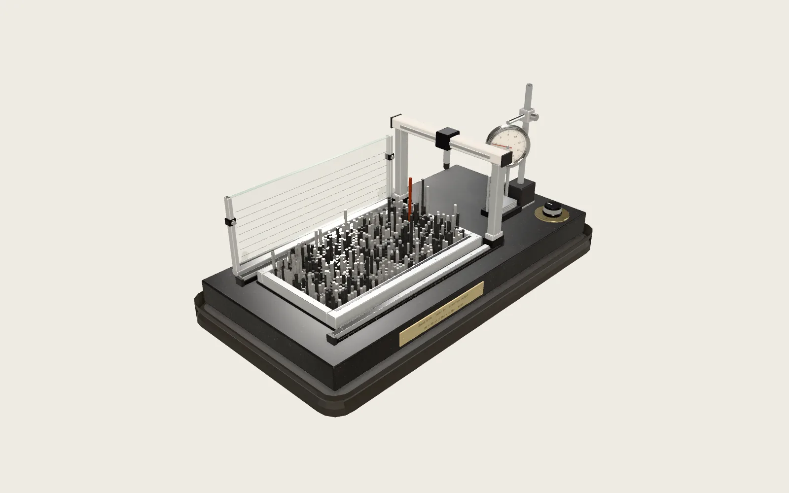 Plate F43LLM QuantizationA language model’s weights are stored with 16 bits each. Quantizing rounds them onto a coarser grid: 8 bits, 4, or only −1, 0 and +1. The model gets several times smaller and faster to read, at a cost in accuracy.